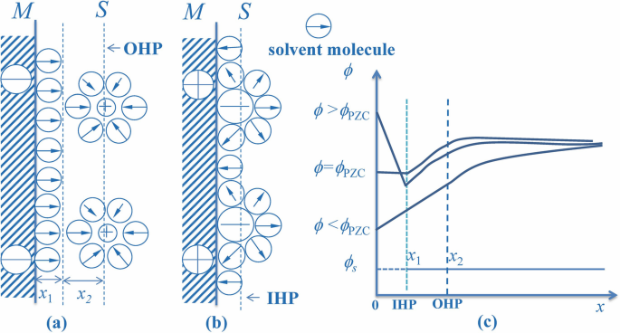
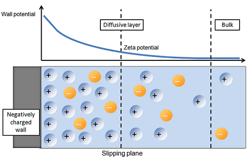
10. Schematic illustration of electrical double layer structure
4.8 (261) In stock

Download scientific diagram | 10. Schematic illustration of electrical double layer structure and the electric potential close to a solid surface with a stern and diffuse layer. Reproduced with permission from Elsevier from ref. [90]. from publication: Development and characterization of new bioactive and antibacterial coatings for biomedical applications using electric field assisted processing | The stability of implants and their long-term survival requires early anchorage at the bone implant interface. This early osteointegration process requires the recruitment of different cells on the periprosthetic site. There is evidence suggesting that a lack of | Zein, Coatings and Antibacterials | ResearchGate, the professional network for scientists.
demonstrates schematic representations of electrical double layer
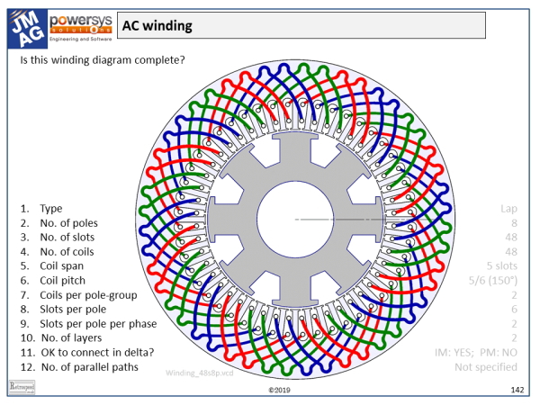
No. 15] Reading a winding diagram Simulation Technology for Electromechanical Design : JMAG

Optical Receiver Design – Fosco Connect

Particle Dispersion for Size Analysis - Particle Technology Labs

Electrochemical Double Layer Capacitors (Supercapacitors)

Jablonski Diagram Notes, Explanation, How to Draw

Electric Double Layer - an overview

Figure 4 from Monolayer Solid-State Electrolyte for Electric Double Layer Gating of Graphene Field-Effect Transistors.
Electrical Double-Layer Structure and Property of Ionic Liquid-Electrode System for Electrochemical Applications

Electrochemical Double Layer - an overview
On the importance of the electric double layer structure in aqueous electrocatalysis
Engineering a passivating electric double layer for high performance lithium metal batteries
Modeling Electroosmotic Flow and the Electrical Double Layer
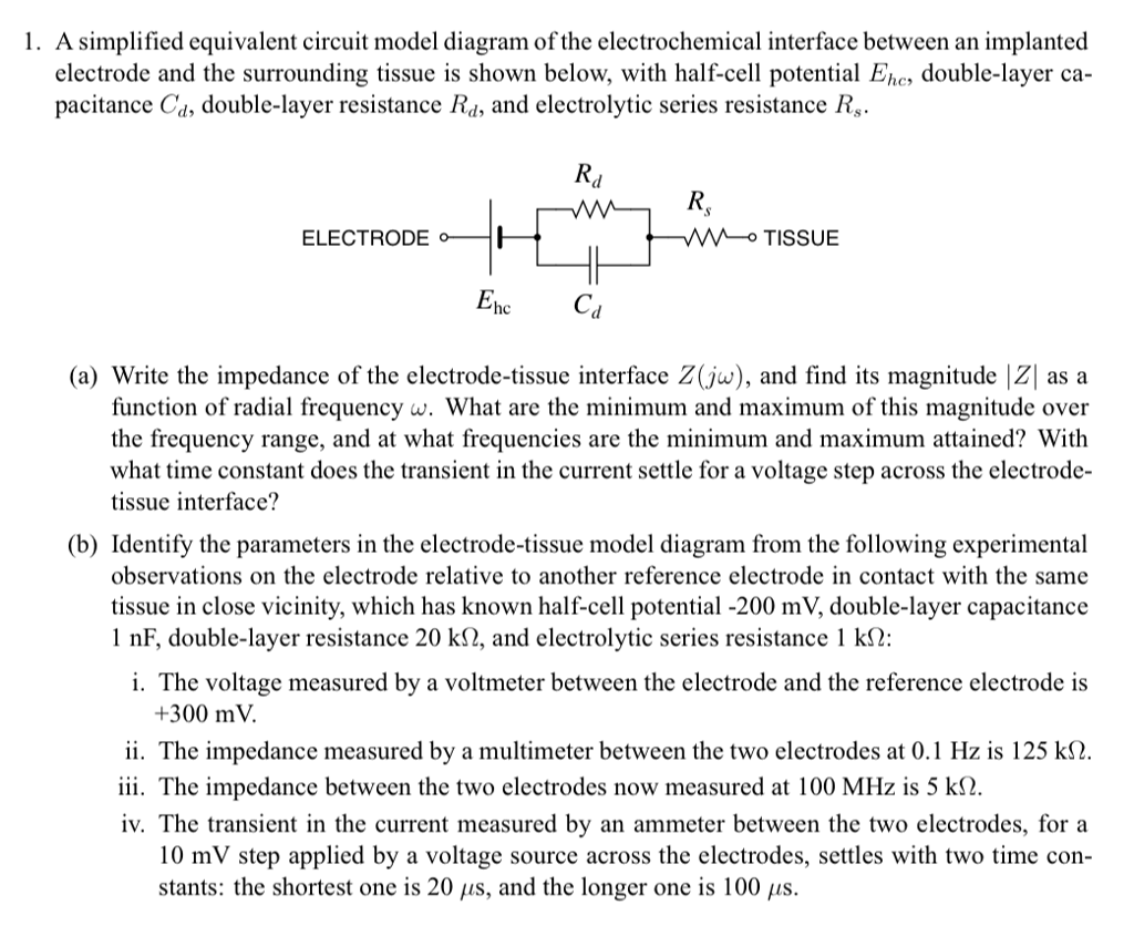
Solved A simplified equivalent circuit model diagram of the
Electric Double-Layer Capacitor (EDLC) How it works, Application & Advantages