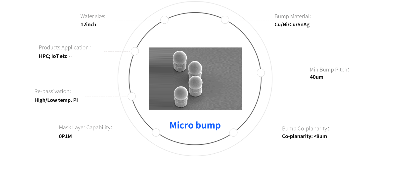
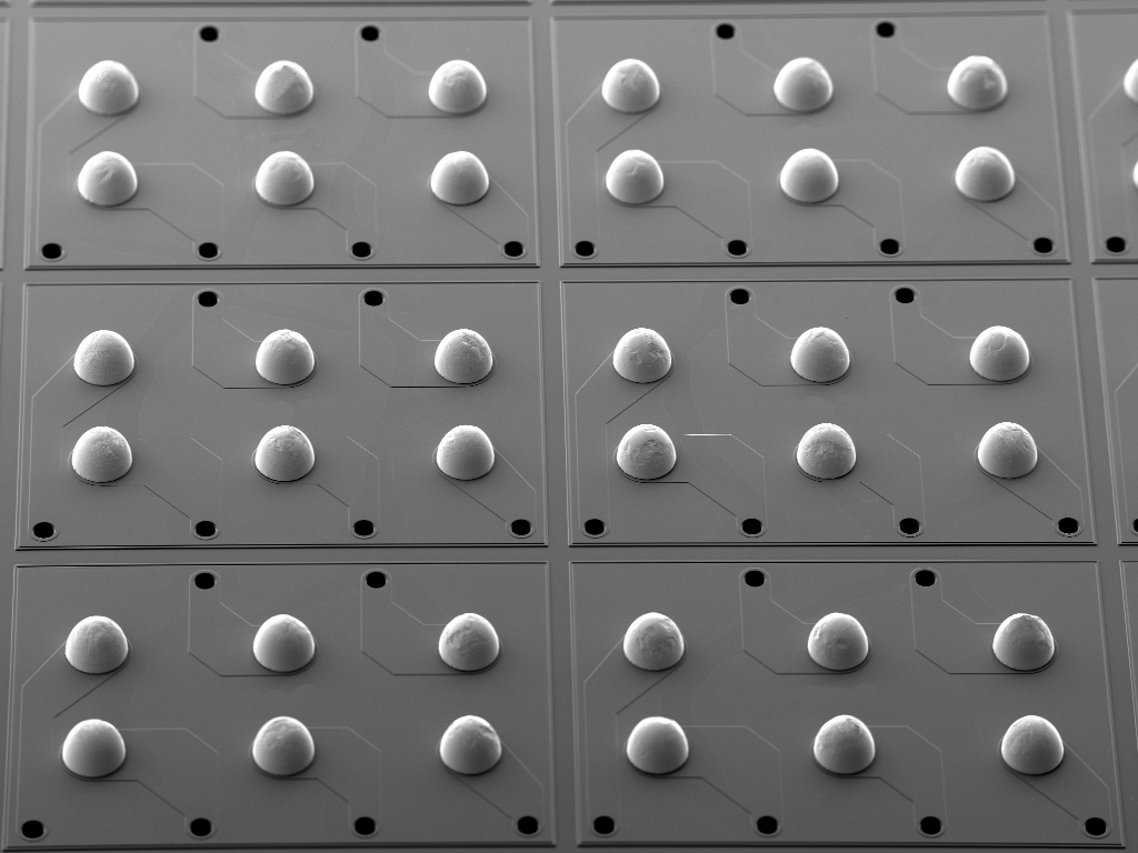
Bump on Pad, Wafer Process Technology
4.7 (446) In stock
Bump on Pad Key features include: Wafer process and bumping in consolidated assembly. Technology supporting wide range of products from mobile devices to
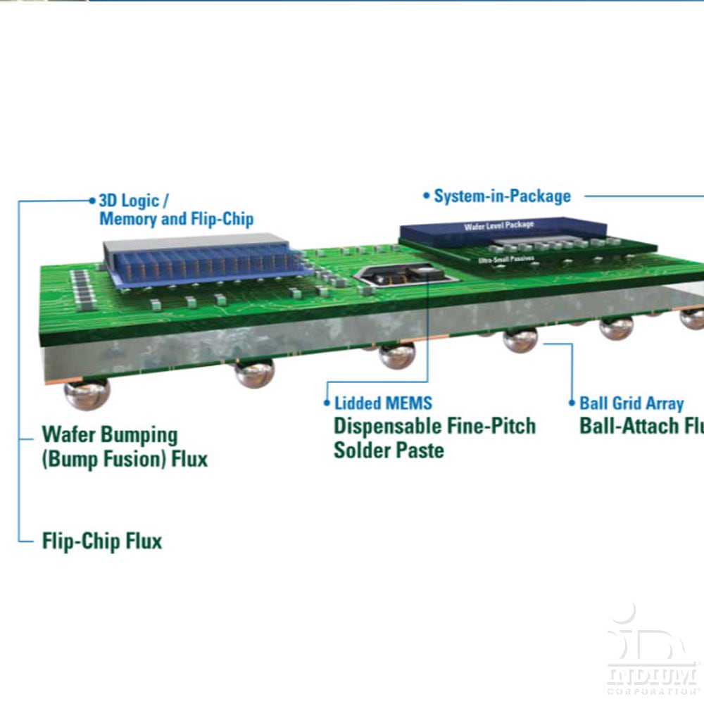
Bump Fusion, Applications

Optimized lithography process flow for creating 6-30 µm bump diameter.
Bump on Pad, Wafer Process Technology
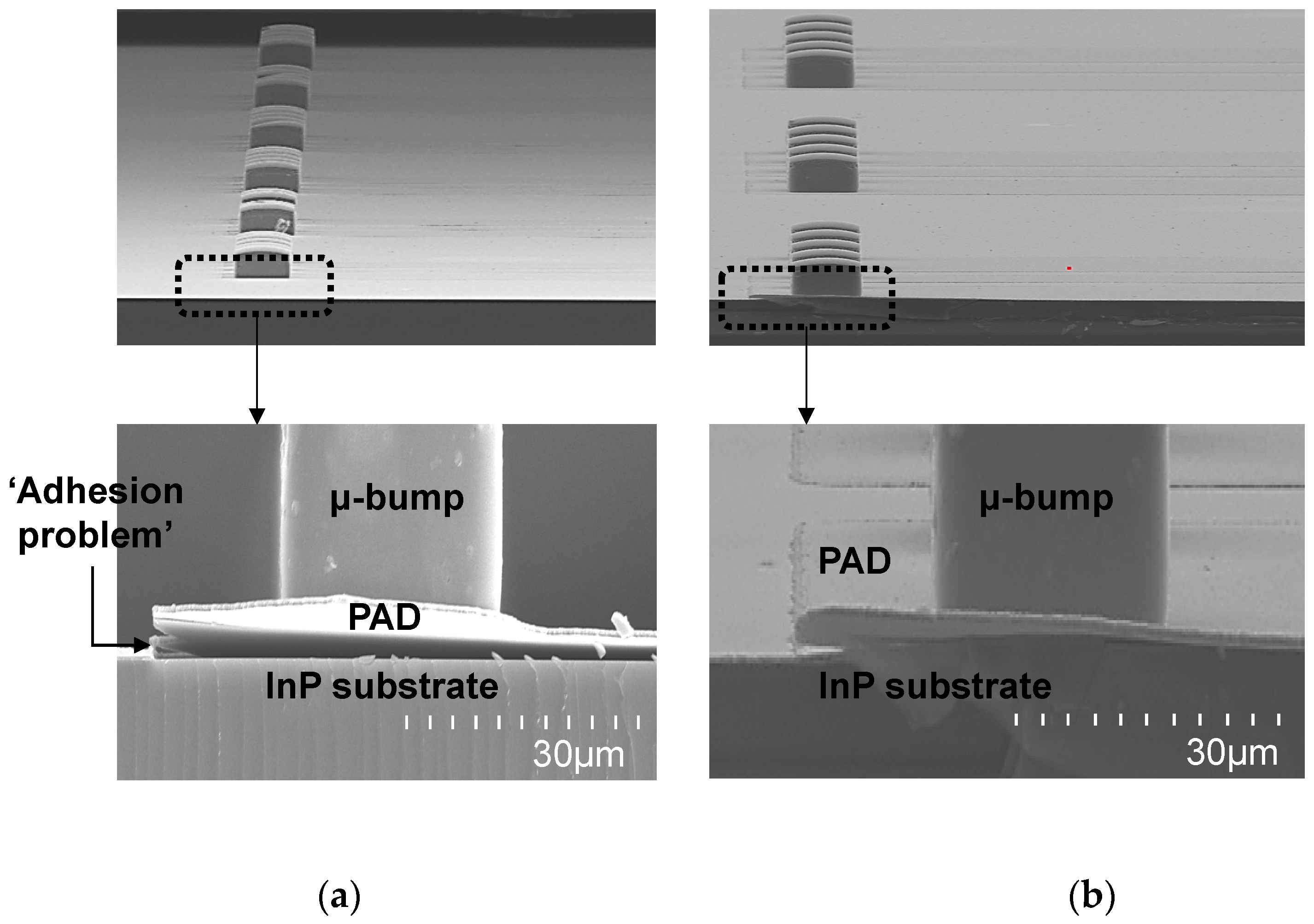
Micromachines, Free Full-Text
Prestige Popular Stainless Steel Pressure Cooker, Litres

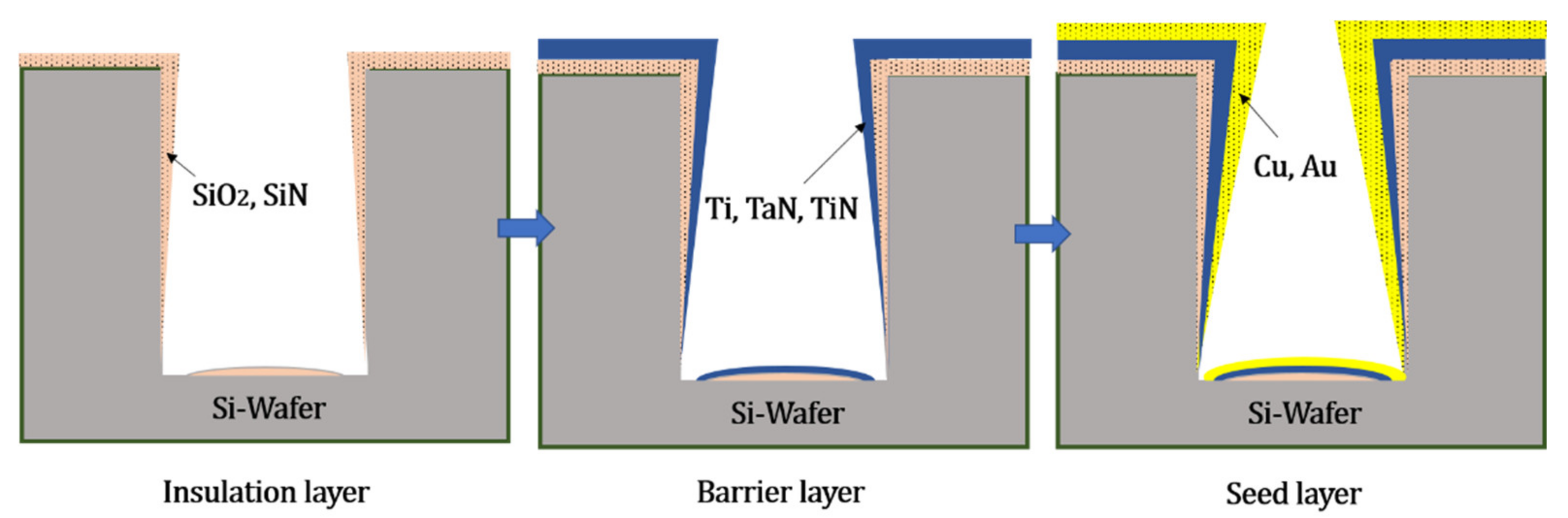
Process and Key Technology of Typical Advanced Packaging
Metals, Free Full-Text

Solder Bump - an overview

Eng Sub] Wafer Level Chip Scale Package (WLCSP)
Wafer Bumping_Wafer Bumping_SERVICE_SJSemiconductor(Jiangyin)Corp.
Solder Balling for WLCSP and Flip Chip Interconnects

Eng Sub] Wafer Bumping Process: Solder bump, Cu pillar bump, UBM
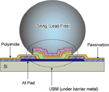
PDF] Under Bump Metallurgy (UBM)-a technology review for flip chip packaging
My dog has bumps under her fur. What is the cause and treatment?
Camburg Toyota Tacoma Pre/4wd 05-23 FOX 2.0 Bolt-on Rear Bump Stop Mount Kit (S/U)
Premium Under Bump Skinny Maternity Jeans
Pregnant Woman Big 9 Month Baby Bump Under White Cloth Stock Image
 NEW! 2021 Barbie Extra Deluxe Doll Pink Shimmer Leggings ~ Pants
 Omkagi Tie Dye Fitness Legging Woman Push Up Workout Sport
 Chicos So Slimming Women's 1.5 (10 US) (32 x 28) Jeans Girlfriend
 Stitched Cotton Kids Fancy Capri Suit, Technics : Woven, Age Group
 Sign Up and get 10% Off – Brastop UK
 Ultrasport Sölden Skihose Damen – Snowboardhose Frauen