PDF] Under Bump Metallurgy (UBM)-a technology review for flip chip packaging
4.8 (547) In stock

Flip chip packaging technology has been utilized more than 40 years ago and it still experiencing an explosives growth. This growth is driven by the need for high performance, high volume, better reliability, smaller size and lower cost of electronic consumer products. Wafer bumping is unavoidable process in flip chip packaging, thus, picking the correct bumping technology that is capable of bumping silicon wafer at high yield and a high reliability with lower cost is challenging. This paper discusses the available wafer bumping technologies for flip chip packaging. The discussion will be focused on process assembly, solder ball compatibility, design structure and lastly cost which translated to overall product costs.

Challenges Grow For Creating Smaller Bumps For Flip Chips

Lost in the advanced IC packaging labyrinth? Know these 10 basic terms - EDN

What are the Advanced Packaging Technologies?

PDF) Under bump metallurgy (UBM) - A technology review for flip

PDF) Pb-free Sn/3.5Ag electroplating bumping process and under bump metallization (UBM)

PDF) Under Bump Metallurgy (UBM)-a technology review for flip chip

PDF) Under Bump Metallurgy (UBM)-a technology review for flip chip
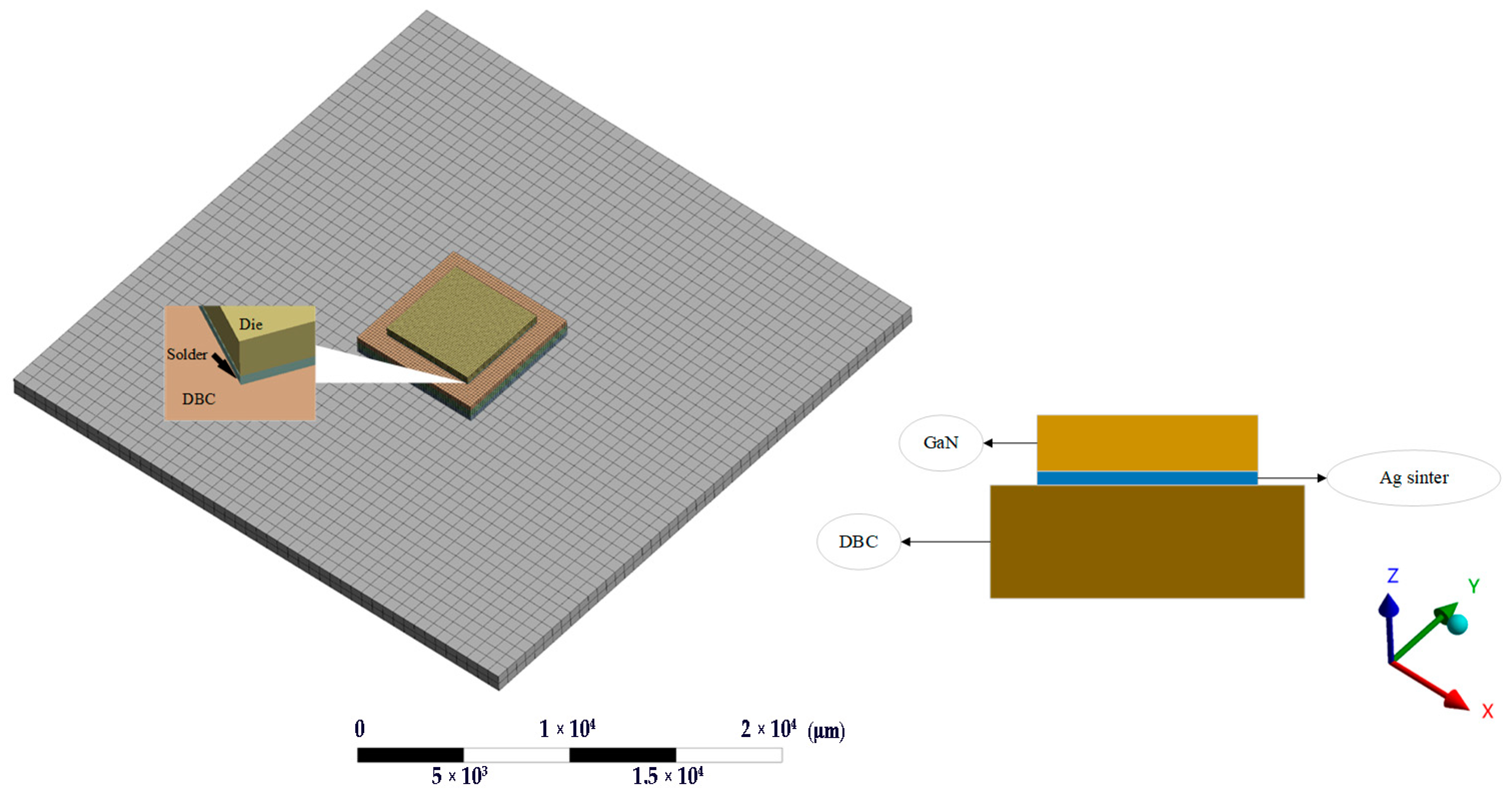
Micromachines, Free Full-Text

Micromachines, Free Full-Text
March - April 2010 - Chip Scale Review

PDF] Under Bump Metallurgy (UBM)-a technology review for flip chip packaging
Figure 2 from Under Bump Metallurgy (UBM)-a technology review for flip chip packaging
Figure 3 from Under Bump Metallurgy (UBM)-a technology review for flip chip packaging
Back Smocked Under Bump Pant – Yo Mama Maternity
Red bump under tongue : r/DentalHygiene
Pregnant Woman Big 9 Month Baby Bump Under White Cloth Stock Image
 Semi Soft Silk Sarees, Naira Cut Kurtis & more, Prashanti
 Koupit Cervicorrect Neck Support Brace for Women Men - Soft
 Elegant Light Blue Lace Bra - H&M Intimates
 Comfort Mesh Fabric Ear Pads for Corsair Virtuoso RGB Wireless SE Headphones Ear Cushions, Cooling Gel Ear Headset Earpads - AliExpress
- Rubbermaid Commercial Slim Jim Recycling Station Black Blue Green 1 Each - Office Depot
 Pockets For Women - Shelter Bay Sleeveless Jersey Midi Dress