Scaling Bump Pitches In Advanced Packaging
5 (508) In stock

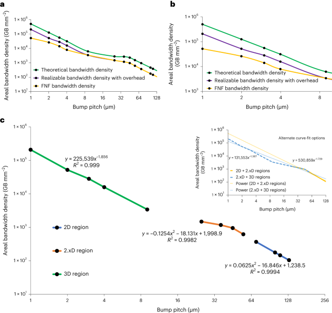
Higher density of interconnects will enable faster movement of data, but there's more than one way to achieve that.

A study of micro-scale solder bump geometric shapes using minimizing energy approach for different solder materials - ScienceDirect

A Broad Look Inside Advanced Packaging

Micromachines, Free Full-Text

Expanding Advanced Packaging Production In The U.S.

Kingston GB DDR4 2133 MHz SODIMM V CL15 260-Pin Notebook, 50% OFF

Heterogeneous Integration and IC Packaging - EE Times Europe

Kingston GB DDR4 2133 MHz SODIMM V CL15 260-Pin Notebook, 50% OFF

Why Advanced Packaging Materials Matter?(Part B)

Marco Mezger on LinkedIn: #interconnects #ic #data #data #technologies #copper…

Marco Mezger on LinkedIn: #interconnects #ic #data #data #technologies #copper…
High-performance, power-efficient three-dimensional system-in-package designs with universal chiplet interconnect express

Marco Mezger on LinkedIn: #interconnects #ic #data #data #technologies #copper…
Inside the iPad 2: Chip brings 50% browsing boost - CNET
Investigation of Pad Cratering in Large Flip-Chip BGA using Acoustic Emission
Apple iPad 10, 10.9 in. 256 GB, Wi-Fi, A14 Bionic Chip with Neural Engine
 Buy Flamingo Print Button Down Shirt & Pyjama Set in White - Satin Online India, Best Prices, COD - Clovia - LS0385Z18
 G-Form Shin Pads Pro-S Vento - White
 BAND-IT CP0399 3/8 Wide x 0.025 Thick 13/16 Diameter, Galvanized Carbon Steel Center Punch Clamp (Pack of 100): Hand Tool Center Punches: : Tools & Home Improvement
 RD Ribbed Thong Bodysuit – Fashion-Sense-Boutique-Canada
 ALO Yoga, Pants & Jumpsuits, Alo Yoga Highwaist Moto Leggings Size Xxs
 Shorts HD Volley Cinza Escuro - HawaiianDreams