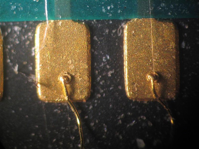
What is a Pad in PCB Design and Development
5 (684) In stock

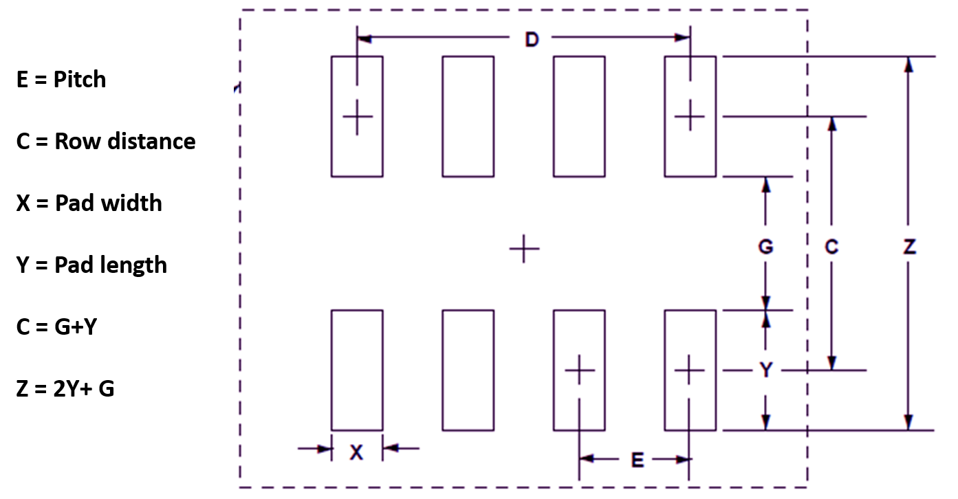
A pad is critical to PCB design as it serves as the designated surface area for electrical contact between the component and the board.
What is a Pad in PCB Design and Development
What is a Pad in PCB Design and Development

PCB Fab Express on LinkedIn: RAPID PROTOTYPE SERVICE
PCB Basic Knowledge_100

PCB Basic Knowledge_84
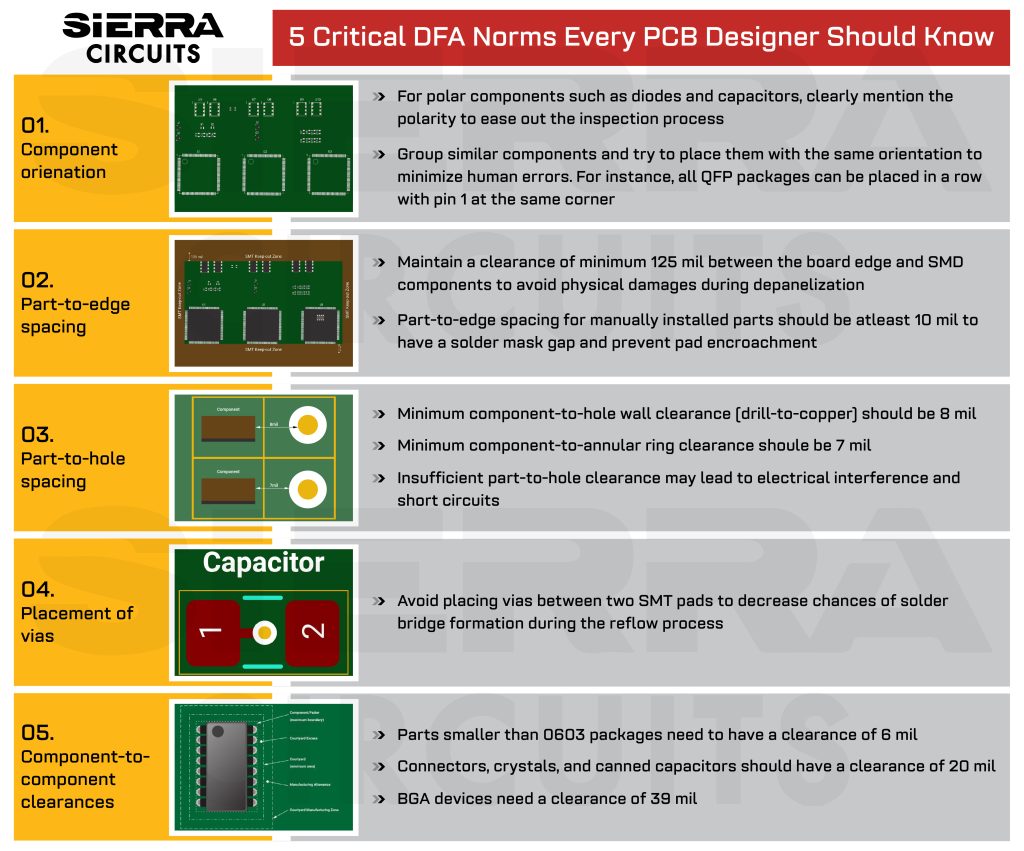
14 Tips For PCB Design For Assembly
PCB Basic Knowledge_84

Component Placement in PCB Design & Assembly

How To Repair Damaged /Missing PCB Pads INVISIBLE Fix, 45% OFF
接触焊点- 维基百科,自由的百科全书
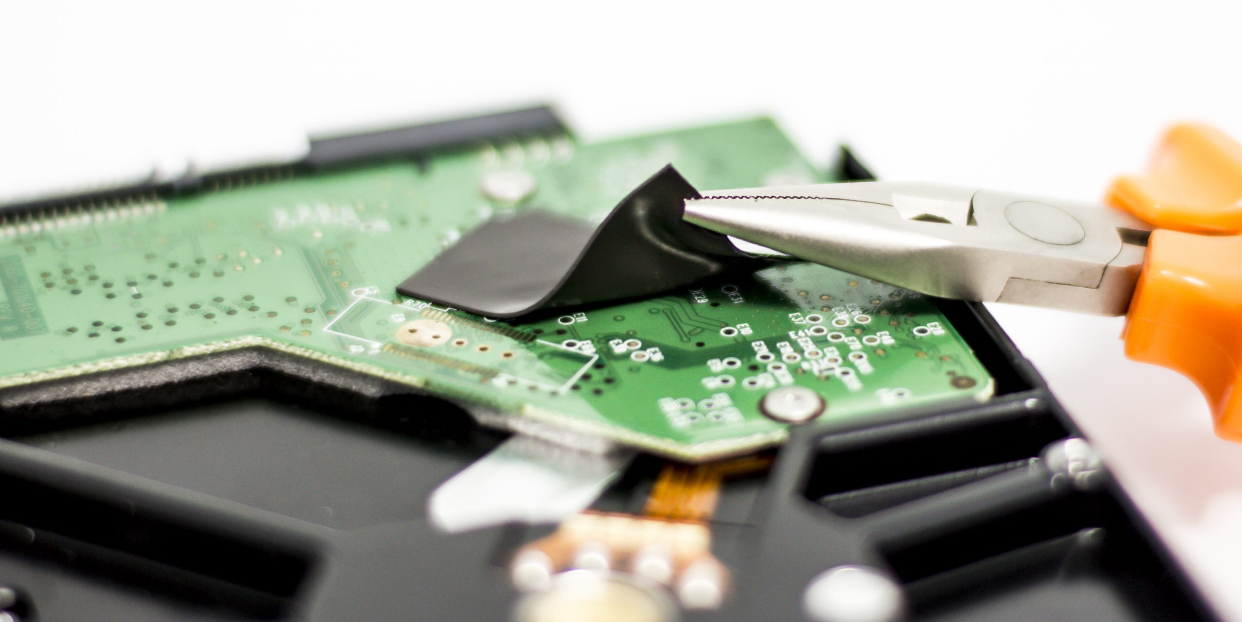
Thermal Pads in PCB Design & Manufacturing

What is a Pad in PCB Design and Development? - Absolute
PCB Basic Knowledge_84

PCB Fab Express on LinkedIn: RAPID PROTOTYPE SERVICE
PCB Basic Knowledge_84
OFFICIAL One Piece Mouse Pads 【 Update March 2024】
Mouse Pad Gamer Speed Extra Grande, 120x60 Cm - One Piece 20 - Faz a Boa!
Japan Anime ONE PIECE Large Mouse Pad Keyboard Desk Mat Pad MousePad
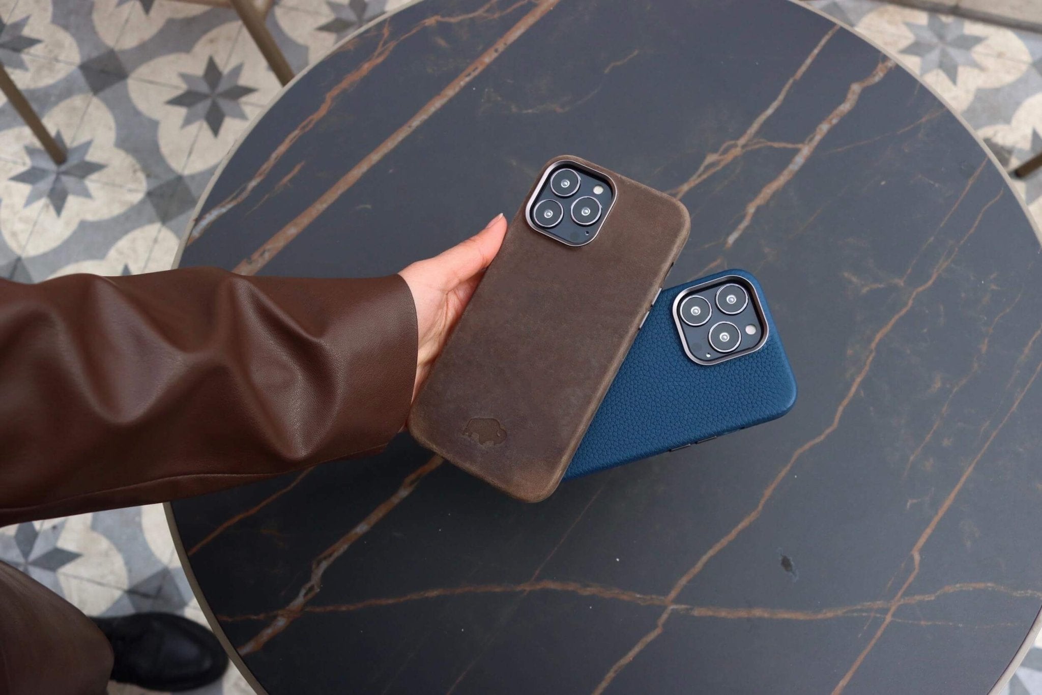 Will Cases Made For the iPhone 13 Pro Fit the iPhone 12 Pro? – BlackBrook Case
 A43 Black Prince Tank UK2' Poster, picture, metal print, paint by
 Perfume ZARA Senhara. FEMME cuspindo perfume fresco 100ml_new
 Stylish Workout Gear for a Sporty Look
 Built-In 360° Long Slip Shaping Maxi Dress
 Welcome - Advantage Fitness Ltd