PDF] Design and Fabrication of Bond Pads for Flip-Chip Bonding of Custom Dies to CMOS Dies
4.6 (677) In stock


PDF] Design and Fabrication of Bond Pads for Flip-Chip Bonding of

PDF) Design and Fabrication of Vertically-Integrated CMOS Image

Wirebonding - Semiconductor Engineering
Electronics, Free Full-Text

Flip-Chip - Semiconductor Engineering
Sensors, Free Full-Text

MEPTEC Report Summer 2018 by MEPTEC - Issuu

CSV CHIP Design Fundamental, PDF, Photolithography

PDF) 3D chip stacking with C4 technology

Application Note: Design and Fabrication of Bond Pads for Flip

Electronics, Free Full-Text

PDF) Direct flip-chip bonding of bare dies to polypropylene-coated paper substrates without adhesives or solders

PDF] Design and Fabrication of Vertically-Integrated CMOS Image
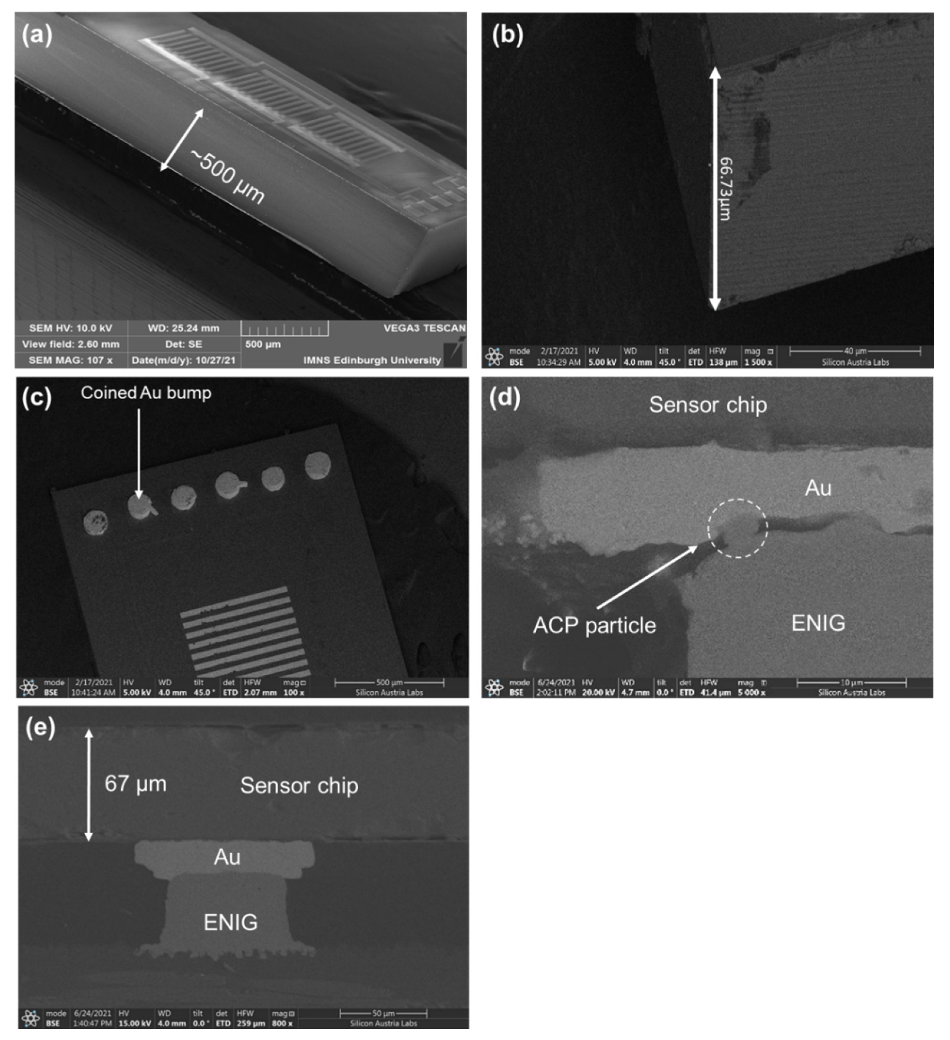
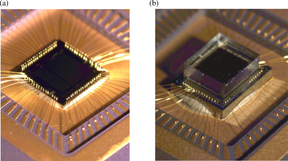
PDF) Die-Level Thinning for Flip-Chip Integration on Flexible

Automated, high-throughput photonic packaging - ScienceDirect
Apple Updates iPad Air With M1 Chip, New Cameras
Gel pad array chip for high throughput and multi-analyte microbead
Schematic of the chip/bump build-up cross-section.
Ingenico IPP350 Credit Card Reader POS Terminal Pin Pad Card Chip Reader
 Wedges Shoes Women High Heels Sandals Summer
 Wingslove Women's Sheer Mesh Bra See Through Sexy Lace Unlined Wireless Plunge Triangle Bras, Lava Red 36D
 Buy Symvi Saree Shapewear Peticote Shapewear for Women Microfiber Saree Shapewear Petticoat for Women, Cotton Blended Shape Wear for Saree (Pink - Mustard - Black, L) Online at desertcartParaguay
 Metallic Leggings-Silver
 New 60 gallon breeder : r/PlantedTank
 Buy Triumph Minimizer 112 Wireless Non Padded Comfort and High