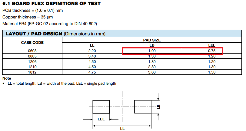
pcb - What is the pad size required for this BGA AW H3 Chip? - Electrical Engineering Stack Exchange
4.9 (456) In stock

I'm trying to figure out the pad size to use for my footprint according to this datasheet.The last page in the datasheet has the package dimensions. I've also posted the relevant information in a p

pcb design - I have a doubt on taking pad dimensions in this below picture what is the pad width and height.any body kindly clear my doubt - Electrical Engineering Stack Exchange

PDF) Complete PCB Design Using OrCad Capture and Layout

863P3 Quad-Band GSM/GPRS module -Model: GE863-PRO3 User Manual Manual Telit Communications S.p.A.

Designing Manufacturable and Reliable Printed Circuit Boards Employing Chip-Scale eGaN FETs
How to Create a SMD pad using the Allegro Padstack Editor? - PCB Design Tutorial - PCBway
pcb - What is the pad size required for this BGA AW H3 Chip? - Electrical Engineering Stack Exchange

pcb design - Recommended Pad Layout Hole Size - Electrical Engineering Stack Exchange

Other Issues - Some Issues concerning BGA(Ball Grid Array)

What is HDI PCB? Application technology of HDI Flex PCB, PCB and PCBA production experts from China

What should be paid attention to in SMT patch processing BGA
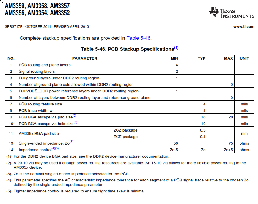
ZCE BGA Pad Size - Processors forum - Processors - TI E2E support forums
Apple unveils new iPad Pro with M1 chip and stunning Liquid Retina XDR display - Apple (CA)
Sigvaris Chip Pads For Lymphedema
Apple Not Giving iPad Wi-Fi Chip Orders To MediaTek, Says Analyst
 Boost Seamless Leggings, Neutral
 Hollister Grand Canyon Arizona Graphic Crew Sweatshirt
 Buy Zivame True Curv Cotton Laminated Non Wired Full Coverage Minimiser Bra - Sundried Tomato2 at Rs.972 online
 luvamia Women's Wide Leg Jeans High Waisted Baggy Jeans for Women
 Los Angeles California - Vintage Sweatshirt for Women Crewneck
 LYOLYTE Racerback Bra, Black