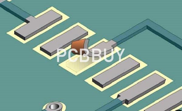
The complete guide to PCB pad :types, size, spacing, repair and
4.9 (95) In stock

Soldering is one of the most important processes in PCBA processing. On printed circuit boards, electrical connections to all components are made via PCB pads. The PCB pads are a very critical part of the PCB that determines where components are soldered on the PCB.The size, shape, and position of pads in a PCB directly depend on the manufacturing quality of the board. Today we will take a look at the PCB pad in SMT soldering.
Soldering is one of the most important processes in PCBA processing. On printed circuit boards, electrical connections to all components are made via PCB pad.

What is a Pad in PCB Design? - JHYPCB

An ultimate guide to PCB gold fingers - IBE Electronics

An ultimate guide to PCB gold fingers - IBE Electronics

The complete guide to PCB pad :types, size, spacing, repair and comparison - IBE Electronics
PCB Pad Size Guidelines with 5 Basic PCB Layout Tips

An ultimate guide to PCB gold fingers - IBE Electronics
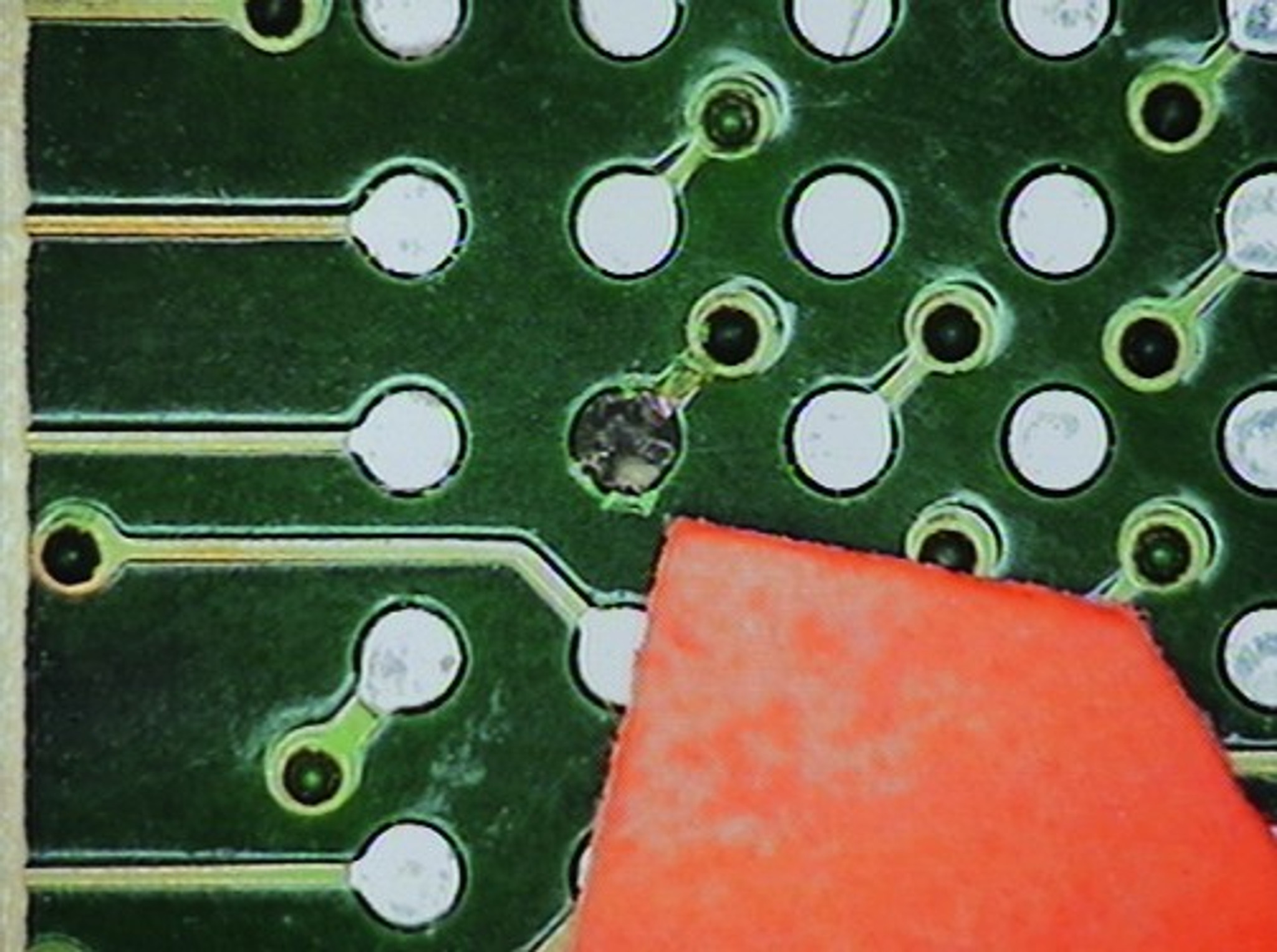
How To Repair Damaged /Missing PCB Pads INVISIBLE Fix, 45% OFF

What is Pad to Pad (PP) ?

What is reflow soldering? Technological process, defects and comparison with wave soldering - IBE Electronics

PCB Via Size and Pad Size Guidelines, by Raymingpcb, Feb, 2024
Shop Best Roofing Pads for Roofing Needs – Roofsmart Pads
Brake Inspection & Repair Service Near Me
Non Slip Furniture Pads - 8 Floor Protectors
 3-6 Women's Sexy NO SHOW SILKY knickers Cheeky Panties Brief Lingerie Underwear
 Luvas Leone 1947 DNA 12 oz
 Olive, Black, or Cabernet Criss Cross Bralette – RockerBelles LLC
 Bragas Control Abdomen Cintura Alta Para Mujer Fajas Corpora
 Calzas Everlast Mujer Por Mayor
 TIYOMI Plus Size 5X Dark Grey Thermal Underwear Suits For Women